Spanish
 Arabic
 French
 Portuguese
 Belarusian
 Japanese
 Russian
 Malay
Malay Icelandic
 Bulgarian
 Azerbaijani
 Estonian
 Irish
Irish Polish
 Persian
 Boolean
 Danish
 German
 Filipino
 Finnish
 Korean
 Dutch
Dutch Galician
 Catalan
 Czech
Czech Croatian
 Latin
Latin Latvian
 Romanian
 Maltese
 Macedonian
 Norwegian
 Swedish
 Serbian
 Slovak
 Slovenian
 Swahili
 Thai
Thai Turkish
 Welsh
Welsh Urdu
Urdu Ukrainian
 Greek
Greek Hungarian
 Italian
 Yiddish
 Indonesian
 Vietnamese
 Haitian Creole
 Spanish Basque

The semiconductor supply chain depends on one constant: uncompromising precision. Every wafer chuck, CVD shower head, test socket, or heat sink that enters a fab must meet tolerances measured in single-digit microns and be produced with repeatability that holds across thousands of units. A single out-of-spec part can bring a lithography line to a halt or scrap a batch of chips worth millions. That is the reality EMAR operates in every day – and it’s why we’ve built our entire CNC Machining ecosystem around the specific needs of semiconductor equipment manufacturers.
This article unpacks the full spectrum of semiconductor parts CNC machining: the techniques that deliver micron-level accuracy, the materials that survive aggressive chemical and thermal environments, the part families that keep fabs running, and the finishing processes that ensure cleanroom compatibility. If you’re sourcing high-precision semiconductor components, you’ll find here a detailed, technically grounded overview of what truly capable manufacturing looks like.
The Precision Imperative in Semiconductor Manufacturing
Semiconductor fabrication has always been a race toward the infinitesimal. What has changed is the manufacturing infrastructure required to support it. As Moore’s Law slows and the industry pivots to advanced packaging, heterogeneous integration, and ever-larger wafer formats, the mechanical components inside process tools are being asked to hold tolerances once reserved for the chips themselves.
Today’s trends only amplify the pressure. Full automation means wafer handling modules and robotic end-effectors need positioning features machined to near-zero deviation. Electrification and the rise of silicon carbide power devices push thermal management components to conduct heat more efficiently than ever. Pervasive digital connectivity and heightened hardware security create demand for test sockets and contactors that can handle thousands of insertion cycles without degradation. Across all these vectors, CNC machining is the common denominator that transforms raw stock into qualified, production-ready parts.
At EMAR, we approach semiconductor work with a single standard: if a feature can be measured, it must be controlled. That philosophy runs through every machine, every process, and every inspection routine on our floor.
Core CNC Techniques for Semiconductor Components
Semiconductor parts span an enormous range of geometries – from cylindrical wafer transport pins to large-format chamber plates with thousands of micro-holes. EMAR deploys a carefully matched set of CNC capabilities to handle that variety without compromise.
CNC Milling (3-axis to 5-axis)
For flatness-critical components such as wafer chucks, gas distribution plates, and polishing pad molds, multi-axis milling provides the combination of surface finish and dimensional control that semiconductor applications demand. Our 5-axis machining centers, including the EMAR VESTA Series and D2-5AX platforms, allow single-setup machining of complex geometries, eliminating stack-up errors that come from multiple fixturing. The result is flatness within ±0.002 mm and surface finishes that require minimal post-processing.
CNC Turning and Swiss Machining
Cylindrical parts – connectors, bushings, wafer transport rollers, and pogo pin housings – are produced on our CNC lathes and Swiss-type automatic lathes. Swiss machining is particularly valuable for the small-diameter, high-length-to-diameter-ratio parts common in test sockets and chip carriers. With sliding headstock technology, we hold diameters to ±0.002 mm on features no larger than a pencil lead.
High-Speed Micro-Machining
Several semiconductor components, most notably CVD shower heads and test sockets, require patterns of hundreds or thousands of tiny holes, each with precise diameter, position, and wall quality. EMAR’s high-speed spindle platforms (up to 60,000 RPM) paired with ultra-low-runout toolholders are purpose-built for this. The low-vibration design preserves tool life over dense hole arrays in stainless steel, brass, and engineering plastics. We also use ethanol-based coolant on these systems – a completely oilless solution that eliminates residue and prevents contamination, making it cleanroom-friendly from the start.
CAD/CAM-Driven Process Control
Every part begins with a 3D CAD model and CAM simulation. Before a single chip is cut, our engineers validate toolpaths, predict material spring-back, and verify clearance for micro-tools. This digital front-end is what allows us to go from a complex, toleranced print to a first-article part with minimal iteration – a critical factor when lead times are tight.
Materials That Meet Fab Requirements
Semiconductor environments are chemically aggressive, thermally dynamic, and relentlessly focused on contamination control. The material palette for CNC-machined components must match those conditions.
Metals
Aluminum alloys (6061-T651, 7075-T651, 5052-T651): Lightweight, excellent thermal conductivity, and naturally corrosion-resistant. Used for heat sinks, handling brackets, wafer chucks, and large structural housings.
Stainless steel (303, 304, 316, 17-4PH): High strength, superior corrosion resistance, and cleanroom compatibility. Deployed in fittings, connectors, gas panels, and chamber components that must withstand aggressive cleaning chemistries.
Titanium (Grade 2, Grade 5): Exceptional strength-to-weight ratio and biocompatibility. Found in specialized wafer handling and medical-semiconductor crossover equipment.
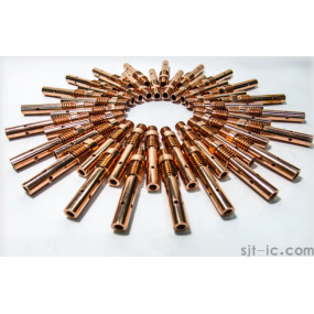
Copper and brass (T2, H59, H62): High electrical and thermal conductivity. Essential for contactors, EMI shielding, and thermal management parts. Brass is also used for connectors where ease of machining and low friction matter.
Engineering Plastics
PEEK: Withstands continuous service temperatures above 250°C, resists virtually all process chemicals, and exhibits extremely low outgassing. The material of choice for wafer handling, insulators, and test sockets.
PTFE (Teflon): Low friction coefficient and universal chemical resistance. Common in seals, gaskets, and insulative components.
Polycarbonate and Delrin (POM): Used for transparent covers, fixtures, and wear-resistant parts where dielectric properties are needed.
Specialized Semiconductor Materials
Beyond standard alloys, EMAR routinely machines substrate-like materials:
Silicon: Semi-crystalline, pure semiconductor material for precision electronic components.
Aluminum Nitride: High mechanical strength combined with thermal conductivity and thermal shock resistance – perfect for heat spreaders and insulating substrates.
Silicon Nitride: Tough, machinable, thermally stable. Used where both electrical insulation and mechanical robustness are required.
This breadth of material competency means you don’t need to qualify multiple suppliers to cover different part families. EMAR handles metal, plastic, and ceramic-like materials under one quality system.
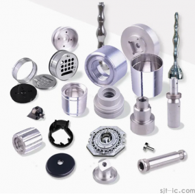
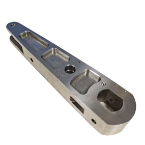
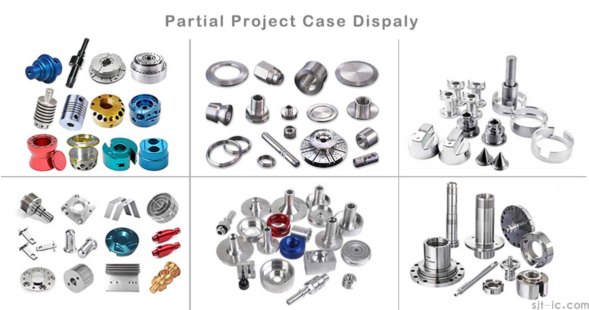
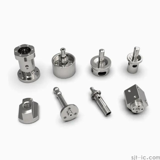
Semiconductor Parts We Manufacture
Over decades supporting the semiconductor industry, EMAR has produced virtually every type of CNC-machined component found in front-end and back-end equipment. Below are the categories that represent the bulk of our daily output.
Wafer Processing Components
Polishing pad molds with precision surface geometries for CMP planarization
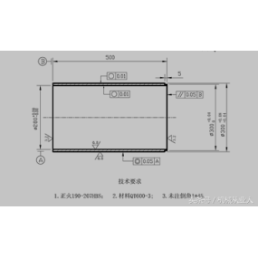
Wafer chucks and carriers, machined flat and parallel to single-digit micron tolerances
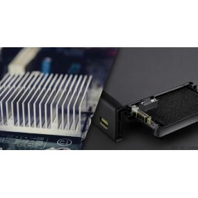
CVD shower heads with dense micro-hole arrays for uniform precursor gas delivery
Gas distribution plates and small wafer chambers (machined on VESTA-1300 platforms)
Wafer conductor processing units and chip-processing plates
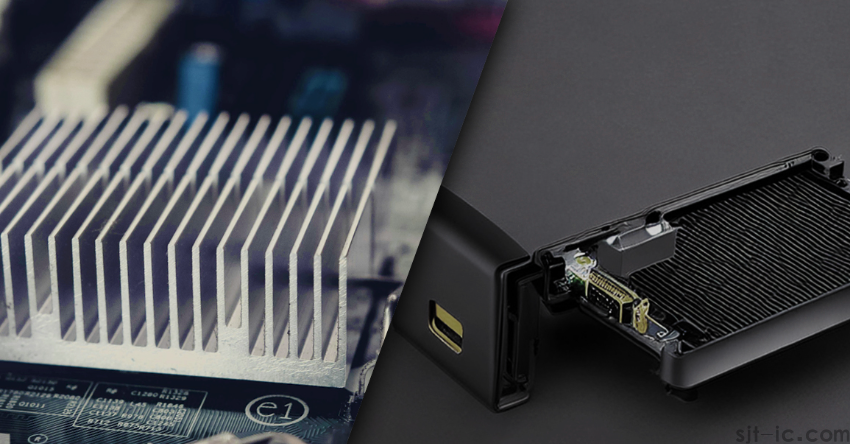
Thermal Management
Aluminum and copper heat sinks with fine-pitch fin geometries
Aluminum nitride thermal spreaders for high-power-density applications
Liquid-cooled cold plates with internal channels
Test, Packaging, and Interconnect
Test sockets with ultra-precise pogo-pin hole arrays machined in PEEK or PEI
Chip carriers and high-density connectors with tight pitch tolerances
Decapsulation fixtures for controlled mechanical chip exposure without damage
PCB rework platforms requiring surgical removal of components on high-value boards
Structural, Handling, and Protection
Wafer handling brackets – rigid yet lightweight, machined from aluminum with vacuum-friendly flatness
Casings, enclosures, and flex circuit stiffeners
Solder paste stencils, gaskets, seals, and insulators
Electromagnetic wafer chucks and fine-line circuit substrates
By keeping all these part families under a single manufacturing roof, EMAR gives equipment OEMs a coherent, scalable supply chain that simplifies vendor management and ensures consistent quality across assemblies.
Surface Finishes for Cleanroom and Performance Demands
A machined part’s surface is its interface with the process environment. The wrong finish can generate particles, trap contaminants, or degrade under chemical exposure. EMAR’s in-house and partner finishing capabilities cover the full range required for semiconductor use.
Anodizing and hard anodizing: Corrosion-resistant, non-conductive coating for aluminum parts. Hard anodizing adds superior wear resistance for moving components.
Micro-arc oxidation: Ceramic-like layer for aluminum, magnesium, and titanium – ideal when extreme hardness and dielectric strength are needed.
Electroless nickel plating: Uniform, corrosion-resistant layer for steel, stainless steel, brass, and copper components, often specified for gas panel fittings.
Passivation: Removes free iron and enhances the natural corrosion resistance of stainless steel – a baseline for any fab-facing part.
Polishing: Delivers smooth, particle-free surfaces that are inherently cleanroom-compatible.
Laser marking: Permanent identification without inks or labels that could outgas or shed particles.
Every finish is selected and applied with an eye toward maintaining the dimensional integrity that was achieved in machining. When a part has been held to ±0.002 mm, the coating process must not undo it.
The EMAR Manufacturing Advantage
We don’t just own machines. We’ve assembled an ecosystem that is designed to de-risk semiconductor component sourcing.
Purpose-Built Machine Portfolio
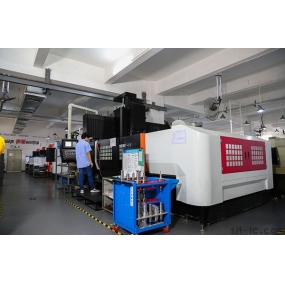
Our floor includes more than 200 CNC machines, among them 5-axis centers (Jingdiao, DMG, AFMING, Roders), Swiss-type lathes (Tsugami, Star), and our proprietary EMAR VESTA and SIRIUS series vertical machining centers. The VESTA-660 and VESTA-1000+ platforms deliver the rigidity, spindle reliability, and thermal stability needed for tight-tolerance, high-volume work. Where part complexity escalates, SIRIUS-UM+ and UL+ machines step in with even faster cycle times and higher dynamic accuracy. The common thread is repeatability: parts cut on one machine match parts cut on another, batch after batch.
Tolerance Framework You Can Rely On
We routinely hold linear dimensions to ±0.01 mm on metals and ±0.05 mm on plastics, with best-case features (diameters, critical holes, parallelism) reaching ±0.001 mm to ±0.002 mm. These aren’t theoretical numbers; they’re verified on Zeiss and Hexagon CMMs, 2.5D vision systems, and XRF spectrometers integrated into our production flow.
Cleanroom-Aware Machining
Our ethanol-cooled high-speed machining cells are designed to produce parts that arrive at your facility clean, with no oily residue. This is particularly critical for components destined for direct wafer contact or vacuum environments.
Engineered Process, Not Just Parts
With 30+ engineers on staff, EMAR provides DFM feedback from the quoting stage. We analyze tolerances, suggest material alternatives where appropriate, and simulate toolpaths before metal is cut. Whether you need five prototypes or 500,000 units per year, the process scales without re-engineering.
Global-Ready Logistics
Located with direct access to major shipping ports, we deliver on DAP or FCA terms with competitive lead times. Our ISO 9001:2015 certification documents the systematic quality management that underpins every shipment.
Bring Your Most Demanding Semiconductor Components to EMAR
When precision is non-negotiable and lead times are tight, you need a CNC machining partner that understands the semiconductor world from the inside out. EMAR combines advanced multi-axis machines, a deep material catalog, cleanroom-compatible finishing, and process discipline to turn your most complex designs into qualified production parts – on time and on spec.
Let’s discuss your next project. Reach out to our engineering team for a technical consultation and quote.
📞 +86 18664342076
📧 sales8@sjt-ic.com
🌐 Visit our website for instant RFQ upload.